Monostable
When a monostable receives an input, the output changes state for a set time and then changes back to its stable state.
There are many different monostable circuits.
A very simple monostable can be made using a logic gate, e.g. a 4093 NAND gate.
The circuit diagram for the simple monostable is shown below.

When the circuit is first switched on, the capacitor is uncharged and so the input to the NAND gate is logic 0.
This makes the output from the NAND gate logic 1.
The input of the circuit is kept at logic 0 by the large value resistor, r. (r is a 'pull down' resistor.)
When the input is taken to a logic 1, the capacitor charges quickly through the diode and the output of the NAND gate becomes logic 0.
When the input returns to logic 0, the capacitor now starts to discharge through the resistor R, until the voltage across the capacitor is just below the lower switching level of the NAND gate.
The input is now a logic 0, the output becomes a logic 1 and the circuit is back in its stable state.
To test the circuit, connect a led and resistor between the output and 0V as in the Introduction page
Use a 1MΩ resistor for R and a 10µF capacitor for C.
Connect the 9V battery and the LED should light.
Touch the input to the positive power supply line, and note what happens.
This monostable circuit has two major problems
– the length and voltage of the input alters the time the output is low,
– the monostable will be restart if the input goes to logic 1.
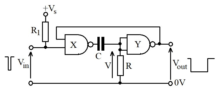
The circuit diagram for an improved monostable is shown below.

The input voltage, Vin, is held at logic 1 by R1.
The inputs of NAND gate Y are held at logic 0 by the resistor R.
Therefore the output, Vout, is at logic 1.
Since both inputs of gate X are at logic 1, the output of X will be at logic 0.
With the capacitor, C, discharged this is a stable state.
Consider what happen when Vin becomes logic 0 for a short time.
The output of X will become logic 1 and the supply voltage will appear across R as the capacitor begins to charge through R.
This makes the input to Y logic 1, so making the output from Y logic 0.
This in turn makes the top input of gate X logic 0 and so will keep the output of gate X at logic 1 even when Vin returns to logic 1.
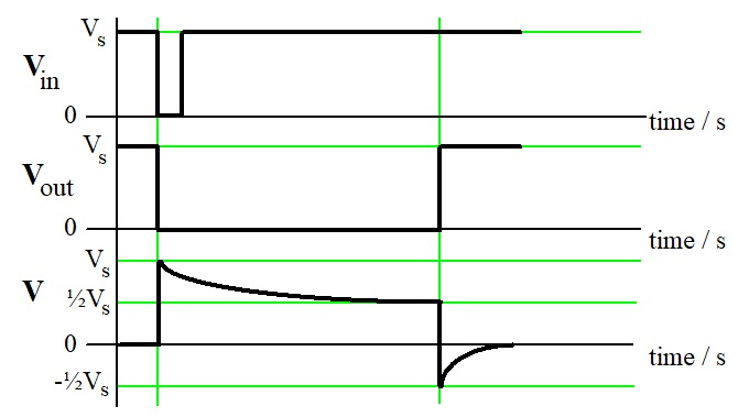
Meanwhile the capacitor is charging through R and as it does, the voltage across R, V, will decrease.
This will continue until V is just below the switching threshold of gate Y, i.e. half of the supply voltage.
When this happens the output of gate Y will become logic 1, which in turn will make the top input of gate X logic 1.
With both inputs to gate X now at logic 1, its output becomes logic 0 and the capacitor discharges as the stable state is again restored.
For the monostable to function successfully, the duration of the input pulse must be shorter than the time period of the monostable.
The duration of the output pulse, in seconds, of the monostable is given approximately by
T = R × C
where C is in farads and R is in ohms.The sketch graphs below show the operation of the monostable.

NAND gate monostables are triggered with 'negative going' pulse, and so are said to be 'falling edge triggered'.