
Astable Oscillator
There are many different oscillator circuits.
An Astable oscillator is a digital circuit with no stable states.
To produce the delay in the digital circuit switching on and off, a capacitor is used.
Capacitor circuit symbol
Capacitor types and uses
A very simple astable oscillator can be made using an inverting logic gate with Schmitt trigger inputs, e.g. a 4093 NAND gate.
The circuit diagram for the astable oscillator is shown below.
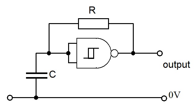
When the circuit is first switched on, the capacitor is uncharged and so the input to the NAND gate is logic 0.
This makes the output from the NAND gate logic 1, and so the capacitor starts to charge through the resistor R.
When the voltage across the capacitor just exceeds the upper switching level of the NAND gate, the input is then a logic 1, and the output a logic 0.
The capacitor now starts to discharge through the resistor R, until the voltage across the capacitor is just below the lower switching level.
The input is now a logic 0, the output becomes a logic 1 and so the process repeats.
The rate at which the output switches between logic 0 and 1 is determined by R and C (as well as the supply voltage and type of logic gate).
To test the circuit, connect a LED and resistor between the output and 0V as in the Introduction page
Use a 1MΩ resistor for R and a 1µF capacitor for C.
Connect the 9V battery and the LED should flash with a period of ≈1.5s. (On ≈0.4s, Off ≈1.1s)
It is useful to examine the voltage across the capacitor and the output voltage with an oscilloscope.
Notice how the voltage across the capacitor varies as the output switches.
The oscillator can be controlled by using one of the NAND gate inputs.
The circuit diagram for the oscillator is shown below.
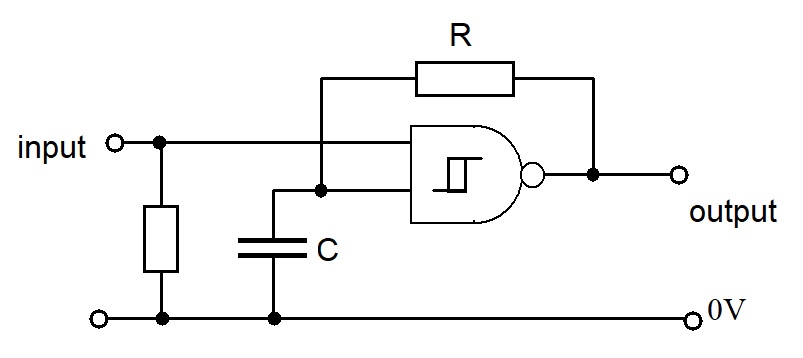
When the input is logic 0, the oscillations stop and the output becomes logic 1.
When the input is logic 1, the oscillations start.
The circuit diagram for this oscillator is shown below.
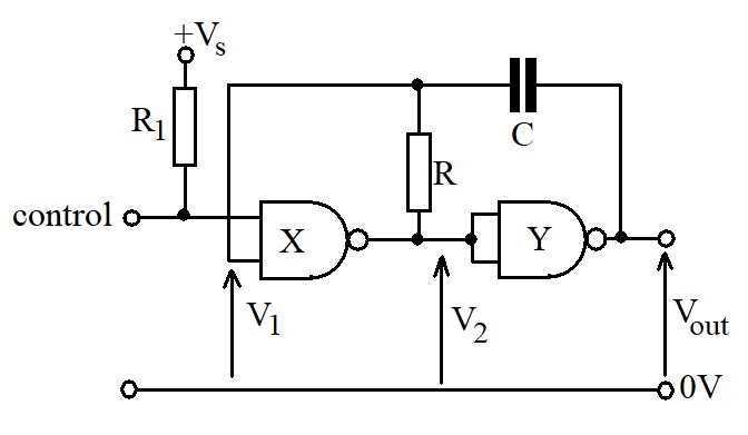
When the astable circuit is switched off, the capacitor is discharged.
When the circuit is switched on and there is no connection to the control input, imbalances between the two NAND gates will ensure that one of the NAND gate outputs will become logic 1.
Assume that gate Y's output becomes logic 1.
This means that the input to gate Y must be logic 0, as must the output of gate X.
This in turn means that the input to gate X must be logic 1, which it will be since the capacitor will be charging through R from the output of gate X.
So the circuit is semi-stable.
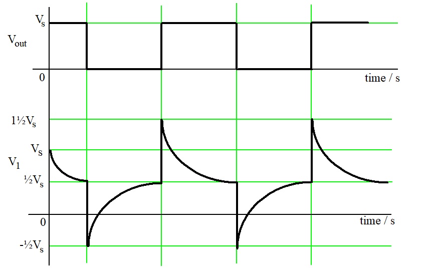
As the capacitor charges, V1 will decrease until it is just less than half of the supply voltage.
When this happens, the input to gate X becomes a logic 0 and so the output of gate X will become logic 1.
This in turn makes the input to gate Y logic 1, so the output of gate Y becomes logic 0.
The voltage that was across the capacitor, as a result of it partly charging, will now be moved down by the supply voltage, Vs, so that V1 = -½Vs (in practice -0.6V).
The capacitor will now charge up in the other direction, through R, until V1 is just greater than +½Vs.
When this happens the input of gate X will be a logic 1, so making its output a logic 0, which in turn will make the output of gate Y logic 1 again.
The capacitor will again have a voltage of ½Vs across it and so when the output of gate Y becomes logic 1,
the voltage levels of the capacitor will be shifted up by Vs so making V1 = 1½Vs (in practice Vs + 0.6V).
The capacitor will now start to discharge through R until V1 falls to just less than ½Vs, and so the whole process repeats.
It should be noted that the initial output pulse is shorter than the consequent pulses due to the fact that the capacitor was initially discharged.
It should also be noted that since the capacitor has to charge up in both directions, electrolytic capacitors are not suitable for this application.
This effectively limits the maximum value of C to 1µF.
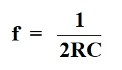
To a first approximation, the frequency of oscillation of the astable is given by
The sketch graphs below show the operation of the astable when there is no connection made to the control input.
The control input provides a convenient way to stop and start a NAND gate astable.
If the control input is at logic 1 the astable operates normally.
If the control input is at logic 0 then the output of gate X becomes logic 1 so making the output from gate Y logic 0 and so stopping the oscillation.
The resistor R1 is a 'pull up' resistor so that if nothing is connected to the control input then it will be held at logic 1.
If the control facility is not required, R1 can be omitted and the two inputs of NAND gate X connected together.