
Enhancement Mode Metal Oxide Semiconductor Field Effect Transistor
(MOSFET)
They have a very large input resistance, (>50MΩ), and a correspondingly large current gain.
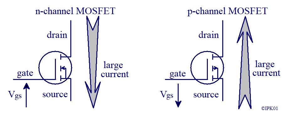
There are two types of MOSFET:-
- n-channel which require a positive voltage input,
- p-channel which require a negative voltage input.
Their symbols and current flow diagrams are shown in the diagram below.
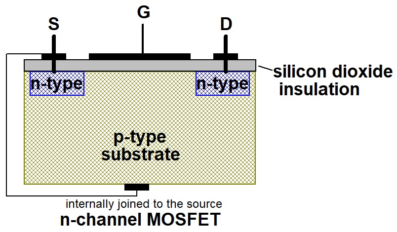
For a drain current to flow, a channel has to be created for the free movement of electrons.
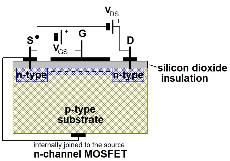
This is achieved by applying a potential difference between the gate and the source, with the gate at the higher potential (VGS).
The silicon dioxide insulator ensures that electrons attracted from the n-type material to the positive gate electrode collect in the p-type substrate beneath the gate electrode.
These electrons begin to fill the holes in the p-type substrate.
As VGS is increased, more electrons collect beneath gate electrode in the p-type substrate until eventually the holes are all neutralised beneath the gate electrode.
The voltage at which this happens is called the Threshold Voltage (VT).
The excess electrons now form an n-type channel between the n-type wells beneath the source and drain, so forming a channel for current to flow from drain to source.
The diagram below shows an n-channel MOSFET arranged as a switch.
The graph shows how Vout varies with Vin.
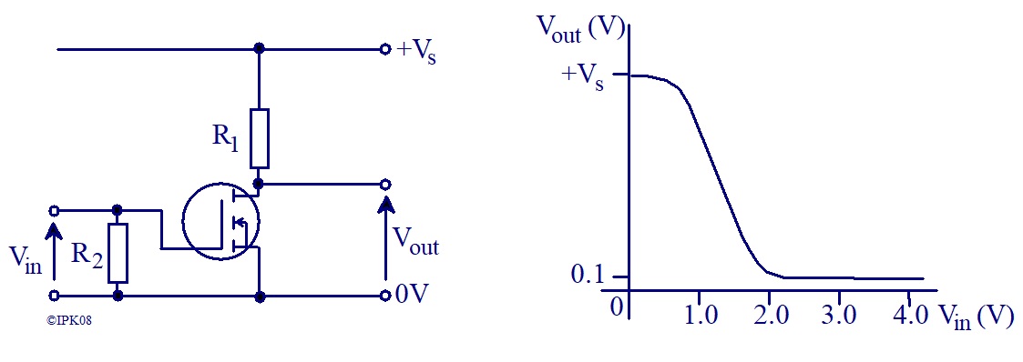
Drain current passes and the MOSFET saturates at about 0.1V, when Vgs is about 2V.
The actual values depend on the type of MOSFET and the drain current passing.
Any further increase in Vin has no effect on Vout.
The MOSFET is therefore operating as a switch in the same way as the transistor.
R2 is not essential and can be omitted - it is only there to ensure that the gate is not able to drift to a large voltage if there is no input.
The value is not critical - 1MΩ to 10MΩ.
There are many different MOSFETs available and the one selected should be able to:-
- operate at the supply voltage (VDS),
- pass sufficient drain current (ID),
- dissipate sufficient power (PD),
- give a very low drain to source resistance (rDS).
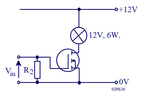
ID ( the drain current) must be greater than 0.5A.
rDS (the drain to source resistance) must be low, preferably less than 0.1Ω.
With a value of rDS = 0.1Ω, the power dissipated is PD = ID2 × rDS = 0.52 × 0.1 = 0.025W
Again, using components that are operating at the limit of their specification leads to poor reliability.
A suitable MOSFET for carrying out the circuit above would be an IRF630 and it is a useful exercise to verify that the specification well exceeds the requirements in this application, though the device is relatively inexpensive.
The main advantages of a MOSFET over a junction transistor are:
- the very large input resistance, (although its impedance at high frequencies can be very low),
- the very large current gain,
- it has a positive thermal coefficient, i.e. if its temperature increases, the resistance from drain to source increases and so decreases the drain current flowing.
As with the transistor switch, if the load is inductive (contains large coils) e.g. a motor, relay, etc, then the MOSFET must be protected from the large voltage that is generated when the current is switched off.
A diode should be connected across the load or from drain to source. See the transistor page
Some MOSFETs have an inbuilt diode connected from drain to source.