
Bipolar Junction Transistors (BJT)
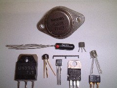
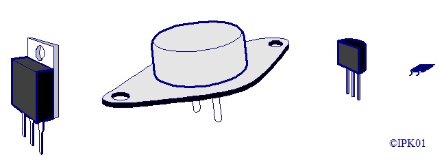
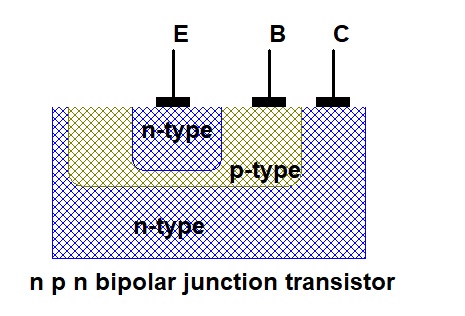
There are two types of junction transistor:-
- npn transistors which amplify a positive current,
- pnp transistors which amplify a negative current.
Their symbols and current flow diagrams are shown in the diagram below.
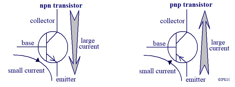
When a small current passes through the base emitter junction a much larger current is made to pass through the collect and emitter.
Since the base emitter behaves as a forward biased diode, for a silicon transistor there will be a voltage of ≈0.7V between the base and emitter.
The diagram below shows an npn transistor arranged as a switch.
The graph shows how Vout varies with Vin.
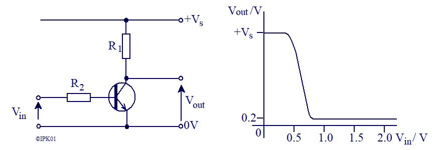
At this voltage a small collector current flows and Vout begins to fall.
When Vin reaches ≈0.7V, the maximum collector current is flowing (limited by R1) and the transistor saturates with a collector-emitter voltage of ≈0.2V.
Any further increase in Vin has no effect on Vout.
The transistor is therefore operating as a switch.
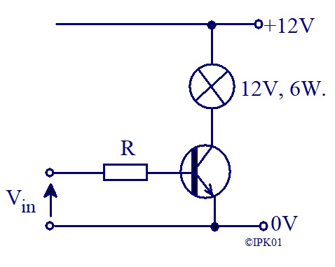
The resistor in the collector circuit, R1, can be replaced with any form of load,
e.g. a 12V, 6W lamp that needs to be switched by a small current, e.g. from a processor
.
Selecting a Transistor
There are many different transistors available and the one selected should be able to:-- operate at the supply voltage (Vce)
- pass sufficient collector current (Ic)
- dissipate sufficient power (Ptot)
- give a large current gain (hFE)
For this example, its Vce (voltage across the collector and emitter) must be greater than 12V.
For a 6W lamp operating on 12V, the current is 0.5A, so its Ic (collector current) must be greater than 0.5A.
When the transistor is switched on, there is approximately 0.2V across the collector and emitter.
The current passing is 0.5A and so the power dissipated by the transistor is 0.2 × 0.5 = 0.1W.
Its Ptot must, therefore, be greater than 0.1W.
Its hFE is a measure of how many times larger the collector current is than the base current.
If possible, a transistor should be chosen so that hFE is greater than 100 at the required collector current.
Using components that are operating at the limit of their specification leads to poor reliability.
A suitable transistor for carrying out the switching function in this example would be a ZTX851, and it is a useful exercise to verify the specifications using a component catalogue. Rapid Electronics
In selecting a suitable value for the resistor in series with the base of the transistor,
sufficient base current needs to pass so that the transistor passes as much as possible, i.e. it is saturated.
However, the resistor needs to prevent too much current from passing so that the base-emitter junction of the transistor is damaged.
As a general rule, a current of up to 5mA can pass into the base of a small junction transistor.
Assuming that the output voltage from the logic gate operating the transistor is 5V, and taking account of the 0.7V across the base-emitter junction of the transistor,
the voltage across R is equal to 5 - 0.7 = 4.3V
Allowing a maximum base current of 5mA, the value of R can be found from Ohm's law.
A suitable base resistor in this application would therefore be 1kΩ
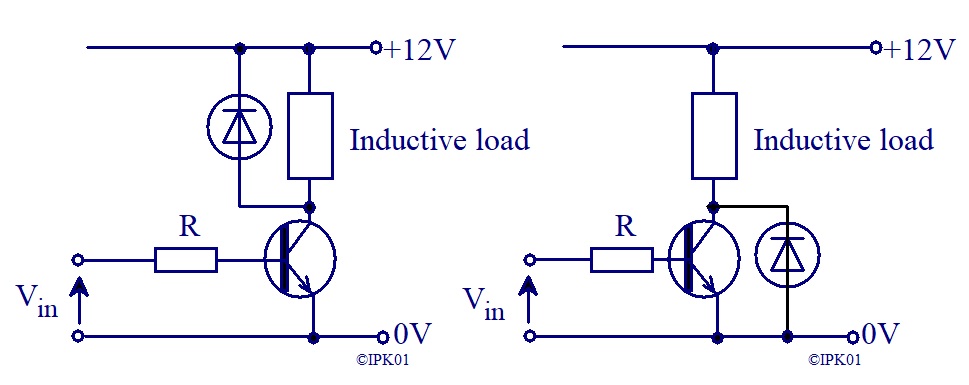
When switching loads containing inductance e.g. motors, relays, solenoid actuators, etc
it is necessary to protect the switching transistor from the large voltage that is produced when the current is switched off.
Failure to do so will result in the transistor driver being damaged/destroyed.
Protection is achieved by connecting a reverse biased diode either from collector to emitter or directly across the load.
The input resistance of a transistor switch circuit is low, i.e. of the order of 1kΩ.
A few mA can provide an unacceptable current drain on some logic circuits.
A better alternative to junction transistors are enhancement mode MOSFETs.