

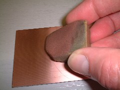
A pcb being cleaned with an abrasive rubber.
Note the polished appearance of the left hand side of the board
which has been cleaned.
When cleaned, the board should be wiped with a degreasing agent e.g. propanone.
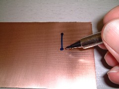
The cleaned pcb can then be drawn on with an etch resistant pen.
It is important not to touch the cleaned board with your hands
because the ink nay not stick to the copper if it is greasy.
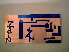
A circuit board ready to etch.
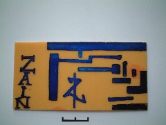
The circuit board etched and ready for drilling.
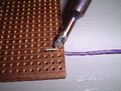
The soldering iron tip warms both the wire and copper track.
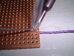
When the wire and track are hot
solder is applied to the tip of the soldering iron.
Note the flux vapour from the solder.
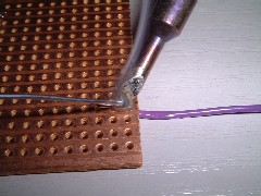
As the solder flows onto the wire and copper track,
sufficient solder is applied to make a strong joint.
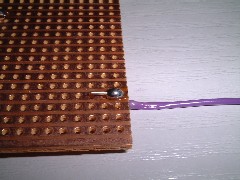
The completed joint is allowed to cool.
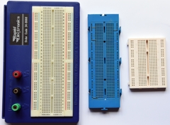
Different types of protoboards.
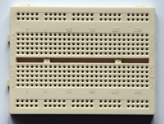
The front of a common type of protoboard.
Note the lugs on the sides of the boards
that enable the them to be joined together.
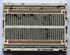
The inside of a protoboard.
Note the metal connectors into which the wires fit.
Note that the top and bottom rows are linked by connectors
and the middle columns are joined, with a gap in the middle.